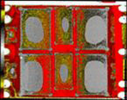
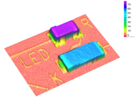
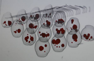
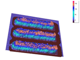
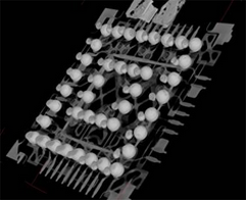
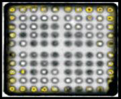
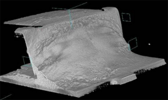
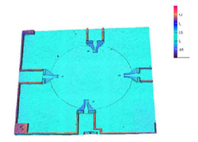
Competence Center for High-resolution Nondestructive Testing
|
Need and requirements for nondestructive testing of electronic components are growing with the increasing complexity of fabrication processes in packaging technology. Complex products have to be transferred to a stable mass production, but on the other hand, highest reliability requirements have to be met for the life cycle of the product. ![]() |
Motivation
The development of nanotechnology and nanoelectronics is dynamically progressing. This dynamics leads to ever more complex but tinier structures and components, which are processed in packaging technology to complex systems.
In future, micro- und nanointegrated systems will penetrate many areas of our life. The tendency of packaging technology towards three-dimensionally integrated system solutions or multifunctional polymer setups brings about a multiplicity of subsequent process steps in the fabrication of electronic components. It has to be taken into account that more and more technologies and processes from the semiconductor industry are applied in packaging technology, e. g. in order to create tiniest connection structures. Fault-freeness of the functional layers used, which are only a few nanometers thick, is codecisive for the quality of the final product. Comparable to semiconductor production, the failure of a single process step causes the malfunction of the whole product. Packaging technology follows this trend. New technologies are developed to control high-pin count contacts, small distances, high power consumption and high frequencies. Such new technologies with big potential are e. g. system-on-chip (SoC), multi-chip-module (MCM), system-in-package (SiP) and system-on-package (SoP), which can be subsumed under hetero system integration. To introduce the new technologies, in order to develop new production processes and their quality assurance, nondestructive testing techniques are needed which are capable of capturing threedimensional structures with nanometer dimension.Mission
Nanoeva, as a center for the nondestructive testing of electronic products, offers enterprises and research institutes - beside services - the development of customized testing devices and training.
The emphasized aim of Nanoeva consists in providing industry with a competent center for development and application of new testing methods, with which new defect types as the transportation phenomenon, re-crystallization, volume modifications, and Kirkendall voids can be resolved. Our customers gain substantial adavantages in competition by the access to most modern testing and analysis equipment. The service offerings are completed by a comprehensive course of seminars and lectures.
